 | –≠–ª–µ–∫—Ç—Ä–æ–Ω–Ω—ã–π –∫–æ–º–ø–æ–Ω–µ–Ω—Ç: PACVGA101 | –°–∫–∞—á–∞—Ç—å:  PDF PDF  ZIP ZIP |

© 2002 California Micro Devices Corp. All rights reserved.
02/14/02
215 Topaz Street, Milpitas, California 95035
L Tel: (408) 263-3214 L Fax: (408) 263-7846 L www.calmicro.com
1
PACVGA100/101
VGA Port ESD Protection and Termination Network
Features
∑
Seven channel ESD protection
∑
+
15 kV ESD protection per channel, connector
side (HBM)
∑
+
8 kV contact, 15 kV air discharge ESD protection
per channel, connector side (IEC 61000-4-2 Level
4 standard)
∑
Low loading capacitance--4.5pF typical
∑
16-pin QSOP package
Applications
∑
ESD protection and termination resistors for VGA
(video) port interfaces
∑
Desktop PCs
∑
Notebook computers
∑
LCD monitors
Product Description
The PACVGA100/101 functions as a transmission line
termination and ESD protection device for video appli-
cations. It provides 75 ohm parallel terminations for
video R, G, and B lines and series terminations for the
Horizontal Sync, Vertical Sync and the two DDC lines
which serve as Plug and Play logic signals. In addition,
all interface lines provide Level 4 ESD protection per
the IEC 61000-4-2 contact discharge specification. The
PACVGA100 provides internal pull-up resistors (R3) for
the two DDC lines whereas the PACVGA101 omits
these internal pull-ups so that different pull-up resistor
values can be added externally.
Simplified Electrical Schematic
Typical Application Circuit
R1 = 75
, R2 = 33
R3 = 2.2K
(for PACVGA100 only)
* R3 omitted for PACVGA101
Red
R1
R2
2
3
5
7
9
11
14
4
13
15
12
10
6
16
8
1
0.2uF
C
BYPASS
V
CC
V
CC
V
i
de
o C
o
nn
ec
t
o
r
V
i
de
o C
o
n
t
r
o
l
l
e
r
R1, R2 required
only for VGA101
H-Sync
V-Sync
DDC_Data
DDC_Clk
Blue
Grn
H-Sync
V-Sync
DDC_Data
DDC_Clk
R
G
B
P
A
C
V
G
A
10
0/
10
1
Note 1: For best ESD protection, minimize R/G/B trace lengths
between the PACVGA100/101 device and the video
(See Note 1)
connector.
© 2002 California Micro Devices Corp. All rights reserved.
2
215 Topaz Street, Milpitas, California 95035
L Tel: (408) 263-3214 L Fax: (408) 263-7846 L www.calmicro.com
02/14/02
PACVGA100/101
PIN DESCRIPTIONS
LEAD(s)
NAME
DESCRIPTION
1, 8, 16
V
CC
Positive voltage supply pins.
2
RGB1
RGB Video Protection Channel 1. Ties to one of the RGB video lines (for example, the
Red signal) between the VGA controller device and the video connector.
3
RGB2
RGB Video Protection Channel 2. Ties to one of the RGB video lines (for example, the
Blue signal) between the VGA controller device and the video connector.
4, 13
V
SS
Ground reference supply pin.
5
RGB3
RGB Video Protection Channel 3. Ties to one of the RGB video lines (for example, the
Green signal) between the VGA controller device and the video connector.
6
SYNC1_CONN
Sync Signal Output 1. Ties to the video connector side of one of the sync lines (for
example the Horizontal Sync signal).
7
SYNC1_CTLR
Sync Signal Input 1. Connects to the VGA Controller side of one of the sync lines (for
example, the Horizontal Sync signal).
9
SYNC2_CTLR
Sync Signal Input 2. Connects to the VGA Controller side of one of the sync lines (for
example, the Vertical Sync signal).
10
SYNC2_CONN
Sync Signal Output 2. Connects to the video connector side of one of the sync lines (for
example, the Vertical Sync signal).
11
DDC1_CTLR
DDC Signal Input 1. Connects to the VGA Controller side of one of the DDC signals (for
example, the bidirectional DDC_Data serial line).
12
DDC1_CONN
DDC Signal Output 1. Connects to the connector side of one of the DDC signals (for
example, the bidirectional DDC_Data serial line).
14
DDC2_CTLR
DDC Signal Input 2. Connects to the VGA Controller side of one of the DDC signals (for
example, the bidirectional DDC_Clk).
15
DDC2_CONN
DDC Signal Output 2. Connects to the connector side of one of the DDC signals (for
example, the bidirectional DDC_Clk).
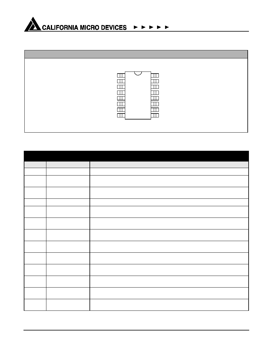
PACKAGE / PINOUT DIAGRAM
Note: This drawing is not to scale.
16-pin QSOP
1
2
3
4
14
13
12
11
5
6
7
10
9
8
15
16
VCC
DDC2_CONN
DDC2_CTLR
VSS
DDC1_CONN
DDC1_CTLR
SYNC2_CONN
VCC
RGB1
RGB2
VSS
RGB3
SYNC1_CONN
SYNC1_CTLR
SYNC2_CTLR
VCC
Top View

© 2002 California Micro Devices Corp. All rights reserved.
02/14/02
215 Topaz Street, Milpitas, California 95035
L Tel: (408) 263-3214 L Fax: (408) 263-7846 L www.calmicro.com
3
PACVGA100/101
Ordering Information
Note 1: Parts are shipped in Tape & Reel form unless otherwise specified.
Specifications
Note 1: Only one diode conducting at a time.
PART NUMBERING INFORMATION
Pins
Package
Ordering Part Number
1
Part Marking
16
QSOP
PACVGA100
PACVGA100Q
16
QSOP
PACVGA101
PACVGA101Q
ABSOLUTE MAXIMUM RATINGS
PARAMETER
RATING
UNITS
Supply Voltage (V
CC
- V
SS
)
6.0
V
Diode Forward DC Current (Note 1)
20
mA
Operating Temperature Range
-40 to +85
∞C
Storage Temperature Range
-65 to +150
∞C
DC Voltage at any channel input
(V
SS
- 0.5) to (V
CC
+ 0.5)
V
Package Power Rating
800
mW
STANDARD OPERATING CONDITIONS
PARAMETER
RATING
UNITS
Operating Temperature Range
-40 to +85
∞C
Operating Supply Voltage (V
CC
- V
SS
)
PACVGA100
PACVGA101
5.0
3.3 to 5.0
V
V

© 2002 California Micro Devices Corp. All rights reserved.
4
215 Topaz Street, Milpitas, California 95035
L Tel: (408) 263-3214 L Fax: (408) 263-7846 L www.calmicro.com
02/14/02
PACVGA100/101
Specifications (cont'd)
Note 1: All parameters specified at T
A
=25∞C unless otherwise noted.
Note 2: These parameters guaranteed by design and characterization.
Note 3: From I/O pins to V
P
or V
N
only; V
P
bypassed to V
N
with 0.2
µF ceramic capacitor.
Note 4: Human Body Model per MIL-STD-883, Method 3015, C
Discharge
= 100pF, R
Discharge
= 1.5K
, V
P
= 5.0V, V
N
grounded.
Note 5: Standard IEC 61000-4-2 with C
Discharge
= 150pF, R
Discharge
= 330
, V
P
= 5.0V, V
N
grounded.
Note 6: These pins are not directly connected to the VGA connector and therefore are not subject to direct ESD strikes.
ELECTRICAL OPERATING CHARACTERISTICS
1
SYMBOL
PARAMETER
CONDITIONS
MIN
TYP
MAX
UNITS
TOL
R
Resistor Absolute Tolerance
R/G/B Termination Resistor (R1)
Series Termination Resistor (R2)
DDC Pull-up Resistor (R3)
+5
+5
+10
%
%
%
TCR
Temperature Coefficient of Resistance (TCR)
+200
ppm/∞C
V
F
Diode Forward Voltage
I
F
= 20mA
0.65
0.95
V
V
RB
Diode Reverse Breakdown Voltage
Top Diode (Cathode connected to V
CC
)
Bottom Diode (Anode connected to V
SS
)
17.0
25.0
V
V
I
LEAK
Channel Leakage Current
+0.1
+1.0
µA
C
IN
Channel Input Capacitance at pins 2, 3, 5, 6, 10, 12 &
15
@ 1 MHz,
V
P
=5V, V
N
=0V,
V
IN
=2.5V; Note
2 applies
4.5
6
pF
V
ESD
ESD Protection
1) Peak Discharge Voltage at pins 2, 3, 5, 6 10, 12
& 15,
in system
a) Human Body Model, MIL-STD-883, Method
3015
b) Contact discharge per IEC 61000-4-2
2) Peak Discharge Voltage at pins 7, 9, 11 & 14
a) Human Body Model, MIL-STD-883, Method
3015
Note 3
Notes 2,4
Notes 2,5
Note 6
Notes 2,4
+15
+8
+4
kV
kV
kV
V
CP
Channel Clamp Voltage at pins 2, 3, 5, 6, 10, 12 & 15
Positive Transients
Negative Transients
@15kV ESD
HBM; Notes 2 &
4
V
P
+ 13.0
V
N
- 13.0
V
V

© 2002 California Micro Devices Corp. All rights reserved.
02/14/02
215 Topaz Street, Milpitas, California 95035
L Tel: (408) 263-3214 L Fax: (408) 263-7846 L www.calmicro.com
5
PACVGA100/101
Mechanical Details
QSOP Mechanical Specifications
PACVGA100/101 devices are packaged in 16-pin
QSOP packages. Dimensions are presented below.
For complete information on the QSOP-16 package,
see the California Micro Devices QSOP Package Infor-
mation document.
* This is an approximate number which may vary.
Package Dimensions for QSOP-16
PACKAGE DIMENSIONS
Package
QSOP (JEDEC name is SSOP)
Pins
16
Dimensions
Millimeters
Inches
Min
Max
Min
Max
A
1.35
1.75
0.053
0.069
A1
0.10
0.25
0.004
0.010
B
0.20
0.30
0.008
0.012
C
0.18
0.25
0.007
0.010
D
4.80
5.00
0.189
0.197
E
3.81
3.98
0.150
0.157
e
0.64 BSC
0.025 BSC
H
5.79
6.19
0.228
0.244
L
0.40
1.27
0.016
0.050
# per tube
100 pieces*
# per tape
and reel
2500 pieces
Controlling dimension: inches
Mechanical Package Diagrams
E
D
H
TOP VIEW
L
END VIEW
C
e
B
A
A1
SEATING
PLANE
SIDE VIEW
5
6
7
8
1
2
3
4
12
11
10
9
16
15
14
13
Pin 1 Marking